
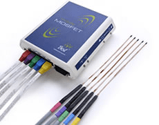
MOSFET Detectors
Metal Oxide Semiconductor Field Effect Transistor (MOSFET) detectors are a semiconductor based radiation detector used for small field dosimetry, in-vivo dosimetry, and profile measurements. The key advantage of a MOSFET detector is the extremely small collecting volume, but the devices are hampered by accumulated damage limiting their effective lives to about 100Gy.
Construction
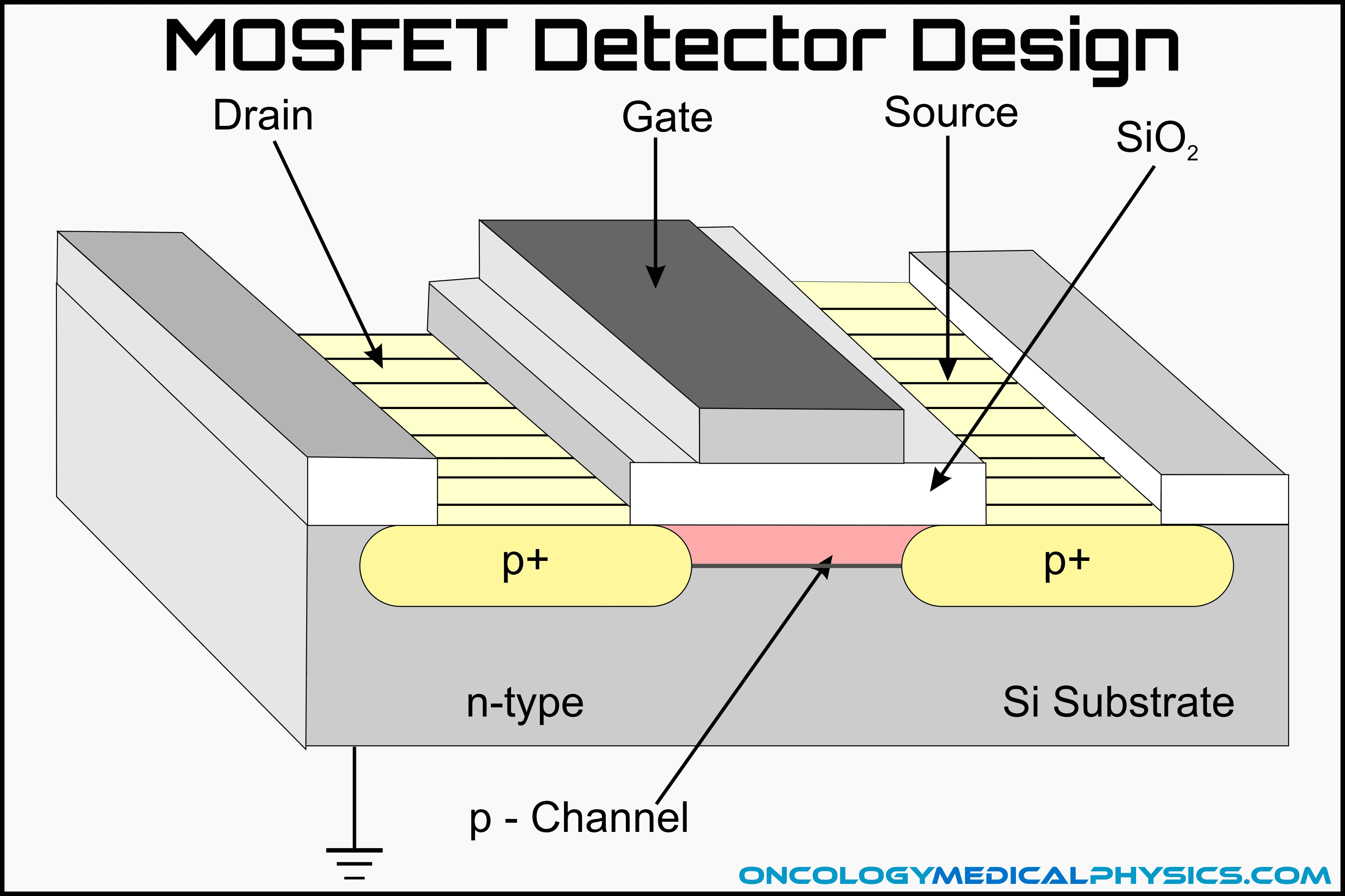
A MOSFET consists of a semiconductor of three leads called the drain, the source and the gate. MOSFETs may be either P-channel or N-channel but P-channel MOSFETs are the most common in dosimeters.
In a P-channel MOSFET, the source and drain are constructed of a P-type (electron acceptor) semiconductor while the gate is constructed of an N-type (electron donor) semiconductor. In an N-channel MOSFET, the construction material types are reversed. The source and drain are embedded in a silicon substrate and are insulated from the gate by a layer of silicon dioxide (SiO2).
The sensitive volume of a MOSFET detector is defined by the silicon dioxide insulator which traps electron-hole pairs during irradiation. Thickness of the silicon dioxide insulator (typically 0.1-1μm) impacts the sensitivity of the MOSFET with thicker layers being more sensitive.
Theory of Operation
A MOSFET can be thought of as a voltage-controlled solid-state switch. When the voltage applied to the gate is too low, the region between the drain and the source contains an excess of electric charge which prevents current flow. When a negative voltage in excess of the threshold voltage is applied to the gate, these electrons are repelled and an inversion layer (sometimes called the channel) forms. This inversion layer allows a current to pass from drain to source.
Note: The above refers to P-channel MOSFET designs which are most common in dosimetry applications. For N-channel MOSFETs, it is excess holes that block the current with VG = 0 and when a positive voltage is applied to the gate (VG > VThreshold) an N-channel forms allowing current to flow.
Dose Measurement
MOSFETs determine dose through measurement in change of threshold voltage as follows:
- As a MOSFET is irradiated, electron-hole pairs are created in the SiO2 layer.
- Holes then migrate to the interface between the SiO2 and the N-type substrate.
- The increase in holes in the interface region retard the electric field induced by applying the negative voltage to the gate. This means that a greater voltage must be applied to the gate to induce current flow between the source and the drain (i.e. it takes a higher voltage to turn the MOSFET on).
- Change in threshold voltage is proportional to the change in number of trapped holes and thus, to absorbed dose.
Key Point: Unlike TLDs or OSLDs which are able to empty their traps, MOSFET detectors accumulate trap filling, reducing their effective usable life to ~100Gy. This property also allows them to act as a persistent dose record.

MOSFET Modes of Operation
Single-bias, single MOSFET: One MOSFET on a chip operated in active mode
- Active mode is applying a negative bias to gate during irradiation
- High temperature dependence
- Sensitivity varies over life of device
Unbiased single MOSFET: One MOSFET on a chip operated in passive mode
- Does not require attached leads during irradiation
- Frequently used as disposable detector
- High temperature dependence
- Instability of response
- Shorter linearity range the biased MOSFET
Dual-bias, dual MOSFET: Two MOSFETs on the same chip operate at different gate biases
- Improves the following
- Improves sensitivity
- Improves reproducibility
- Improves stability
- Reduces temperature dependence
Comparison of Common Dosimeters
| Device -Accuracy | Common Uses | Advantages | Limitations |
|---|---|---|---|
| Ion Chambers ±1% | -Reference Dosimetry -Percent Depth Dose Distributions | -Best understood -Sub 1% accuracy possible -Low energy dependence | -Size limitations -ADCL calibration required |
| Diode Detectors ±2-3% | -Small field dosimetry -Array devices -Electron PDD | -Small volume -Rapid readout -No external bias | -Temperature dependence (0.5%/C) -Dose rate dependence -Energy dependence |
| Film ±2-5% | -Planar dose distributions -Electron PDD | -Best spatial resolution (μm) -Large area measurement -Persistent dose record -Tissue equivalent (radiochromic only) | -Delayed readout -Batch-to-batch variation -Chemical development (radiographic only) |
| Luminescent Dosimeters ±3% | -In Vivo Dosimetry -Personnel dosimeters -End-to-end testing (IROC) | -Small size -Low MV energy dependence | -Delayed readout -Signal loss over time -Supralinear response with accumulated dose |
| MOSFET Detectors | -In vivo dosimetry -Small Field Dosimetry -Surface dose | -Extremely small effective volume -Permanent dose record -Instant readout | -Finite life (~100Gy) -Energy Dependence -Temperature Dependence -Sensitivity changes with accumulated dose |
| Plastic Scintillators | -Small Field Dosimetry -Array Measurements -Electron measurements | -Small volume -Near water equivalent -Dose and rate independent | -Noise, especially Cherenkov Radiation -Sensitivity change with plastic yellowing -New technology, few vendors |
Navigation


Not a Member?
Sign up today to get access to hundreds of ABR style practice questions.